Abstract
Optical experiments on electric field tunable AlAs/GaAs coupled quantum wells clearly demonstrate that the optical nature of these structures can be directly controlled by an applied electric field. In this work we are concerned with calculation and analysis of the first electron and holOe states in these structures. We take into account the effects of the heterostrucuture geometry and of the external uniform electric field applied perpendicularly to the layers, which may lead to an anticrossing of low-lying electron levels in the system. Calculations are performed within the tight-binding supercell formalism with interactions between atomic orbitals up to second nearest-neighbors. Our results show that for GaAs layers less than <img src="http:/img/fbpe/bjp/v32n2a/a18img01.gif" align="absMiddle"> 30 Å wide, application of electric fields takes the structures from typeII to type I heteroestructure behavior. Our estimated value of the electric field intensity needed to cause this transition is in good agreement with the experimental results for comparable heteroestructures geometries .
a18v322a
Electric-Field Effects on the Band-Edge States of GaAs/AlAs Coupled Quantum Wells
F.J. Ribeiro, R.B. Capaz, and Belita Koiller
Instituto de Física, Universidade Federal do Rio de Janeiro, Caixa Postal 68528,
Rio de Janeiro, RJ, Brazil, 21945-970,
Received on 23 April, 2001
Optical experiments on electric field tunable AlAs/GaAs coupled quantum wells clearly demonstrate that the optical nature of these structures can be directly controlled by an applied electric field. In this work we are concerned with calculation and analysis of the first electron and holOe states in these structures. We take into account the effects of the heterostrucuture geometry and of the external uniform electric field applied perpendicularly to the layers, which may lead to an anticrossing of low-lying electron levels in the system. Calculations are performed within the tight-binding supercell formalism with interactions between atomic orbitals up to second nearest-neighbors. Our results show that for GaAs layers less than
30 Å wide, application of electric fields takes the structures from typeII to type I heteroestructure behavior. Our estimated value of the electric field intensity needed to cause this transition is in good agreement with the experimental results for comparable heteroestructures geometries .
Ingenious experimental studies in GaAs/AlAs heterostructures involve the electric-field induced change in optical behavior of these systems. The typical signature of this change is a dramatic increase in the photoluminescence intensity as the main gap of the system changes from indirect to direct under the action of an applied uniform electric field. Examples of investigated structures are coupled quantum wells (CQW) [1,2] and superlattices [3]. Suggested applications for this effect include optical switches, condensation of indirect excitons, analysis of interface quality. Within the effective-mass framework, this effect is qualitatively described by a conduction-band crossing between a level of G symmetry, mainly localized within the GaAs region, and a level of X symmetry, localized within the AlAs.
From the theoretical point of view, the treatment of this problem in the envelope-function effective-mass approximation requires inclusion of the four relevant k-space points in the formalism, one G and the three X points. [4,5,6]. These treatments naturally involve an additional parameter, namely the G-X coupling, which emerges from the broken 3-D translational symmetry of the zinc-blende heterostructure constituents. This parameter is strongly dependent on the geometry of the system [7]. Moreover, inclusion of an external electric field also affects its value.
We present here a tight-binding (TB) treatment for this problem, which includes the heteroestructure geometry and the external applied field. The only input parameters involve the binary constituent components, and couplings due to the reduced symmetry are naturally incorporated in the treatment. An external uniform electric field, applied perpendicularly to the layers, drives the anticrossing of the G-X levels in such structures. In the absence of the applied field, the Hamiltonian is written as

where i,j denote atomic sites in a tetragonal supercell with periodic boundary conditions, and m,n represent the atomic orbitals. We adopt a {sp3s*} basis set and the first- and second-nearest-neighbor TB parametrization proposed by Boykin [8]. This parametrization yields realistic descriptions for the GaAs and AlAs band structures, in particular around the relevant k-points G and X. At each site, the parameters in (1) are taken according to the atomic species occupation [9]. The external field F, applied along the heterostructure growth direction z, is incorporated by modifying the on-site energies [10]

We focus on the lowest electron and hole states in electric-field tunable AlAs/GaAs CQW structures. Following Ref. [1], the active part of the structure consists of 20Å (7ML) GaAs and 40Å (17ML) AlAs, surrounded by wide AlxGa1-xAs barriers. The alloy region is treated within the virtual crystal approximation. Fig. 1(a) shows the ground and excited electron states corresponding to this geometry in the absence of applied field: Note that the ground state is predominantly located in the AlAs region, while the excited state is in the GaAs layer. Fig. 1(b) shows the ground electron state for zero field and under an applied field of 70kV/cm. Comparison of the ground state under applied field with the excited state shown in (a) shows that the applied field inverts the ordering of the two states presented there, thus indicating level crossing takes place.
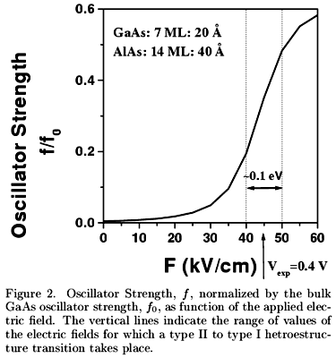
In Fig. 2 we present the optical signature of this crossing, through the calculated oscillator strength of the transition between the first electron and hole states as the applied field increases. Note that the value of the field for which the optical behavior crosses over from indirect to direct is in excellent agreement with the experimental value, ~ 45 kV/cm. This behavior differs from the transition driven by applied pressure in GaAs or by substitution of Ga by Al in AlxGa1-xAs alloys as x increases, which are abrupt, leading to a discontinuous change in the oscillator strength from zero to finite values [11]
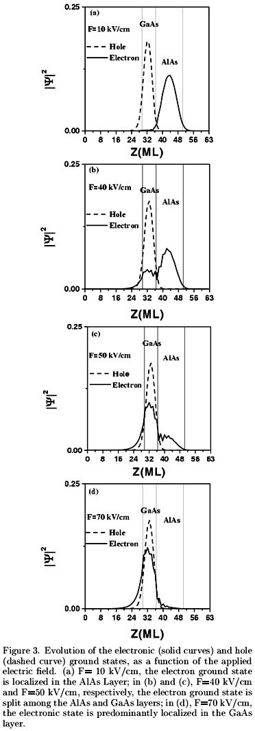
The smooth transition obtained here is typical of level anti-crossing, and may be qualitatively understood from the real space behavior of the electron and hole states as the external field increases, presented in Fig. 3.
Summing up, the TB formalism provides a simple and reliable tool for the treatment of heterostructures under applied electric fields. For GaAs/AlAs coupled quantum wells, the electric fields switches smoothly the system from indirect (type II) to direct (type I) optical regime. The smooth transition, due to the G-X coupling, is understood from the real space behavior of electron and hole states as the electric field switches the system between the two regimes. The calculated value of the switching electric field is in good agreement with experiments performed with the same heterostructure geometry we have considered here.
Acknowledgments
We acknowledge fruitful discussions with T. G. Dargam. This work is partially supported by Brazilian agencies Conselho Nacional de Desenvolvimento Cientí fico e Tecnológico (CNPq), Fundação de Amparo à Pesquisa do Rio de Janeiro (FAPERJ), Fundação Universitária José Bonifácio (FUJB) and Pronex-MCT.
- [1]L. V. Butov, A. Zrenner, G. Abstreiter, G. Bohn, and G. Weimann, Phys. Rev. Lett. 73, 304 (1994).
- [2]A. Zrenner, L. V. Butov, M. Hagn, G. Abstreiter, G. Bohn, and G. Weimann, Phys. Rev. Lett. 72, 3382 (1994).
- [3]M. H. Meymadier, R. Nahory, J. M. Worlock, M. C. Tamargo, and J. L. de Miguel, Phys. Rev. Lett. 60, 1338 (1988).
- [4]T. Ando, and H. Akera, Phys. Rev. B 40 11619 (1989).
- [5]Jian-Bai Xia, Phys. Rev. B 41 3117 (1990).
- [6]Y. Fu and M. Willander, Phys. Rev. B 47 13498 (1993).
- [7]J. G. Menchero, B. Koiller, and R. B. Capaz, Phys. Rev. Lett. 83, 2034 (1999).
- [8]Timothy B. Boykin, Phys. Rev. B 56 9613 (1997).
- [9]J. G. Menchero, T. G. Dargam, and B. Koiller, Phys. Rev. B 61 9613 (200).
- [10]M. Graf and P. Vogl, Phys. Rev. B 51 4940 (1995).
- [11]B. Koiller, and R. B. Capaz, Phys. Rev. Lett. 74, 769 (1995).
Publication Dates
-
Publication in this collection
26 Nov 2002 -
Date of issue
June 2002
History
-
Received
23 Apr 2001