
Abstracts
This paper describes the modeling and control of a three-phase grid-connected converter fed by a photovoltaic array. The converter is composed of an isolated DC-DC converter and a three-phase DC-AC voltage source inverter The converters are modeled in order to obtain small-signal transfer functions that are used in the design of three closed-loop controllers: for the output voltage of the PV array, the DC link voltage and the output currents. Simulated and experimental results are presented.
grid-connected; photovoltaic; converter; PV
Este artigo descreve a modelagem e o controle de um conversor trifásico conectado à rede alimentado por um conjunto fotovoltaico. O conversor é composto de um estágio CC-CC isolado um estágio CC-CA. São obtidas funções de transferência com as quais são projetados três sistemas de controle em malha fechada: um para a tensão de entrada do arranjo de painéis solares, um para a tensão do do barramento de tensão contínua e outro para as correntes trifásicas de saída.
conversor; fotovoltaico; conectado à rede
ELETRÔNICA DE POTÊNCIA
Modeling and control of a three-phase isolated grid-connected converter for photovoltaic applications
Modelagem e controle de um conversor trifásico conectado à rede para aplicações fotovoltáica
Marcelo Gradella VillalvaI; Marcos Fernando EspindolaI; Thais Gama de SiqueiraII; Ernesto RuppertI
IUNICAMP - University of Campinas, Brazil; mvillalva@gmail.com; marcos.espindola@gmail.com; ruppert@fee.unicamp.br
IIUNIFAL - University of Alfenas at Poços de Caldas, Brazil; thaisgama@gmail.com
ABSTRACT
This paper describes the modeling and control of a three-phase grid-connected converter fed by a photovoltaic array. The converter is composed of an isolated DC-DC converter and a three-phase DC-AC voltage source inverter The converters are modeled in order to obtain small-signal transfer functions that are used in the design of three closed-loop controllers: for the output voltage of the PV array, the DC link voltage and the output currents. Simulated and experimental results are presented.
Keywords: grid-connected, photovoltaic, converter, PV
RESUMO
Este artigo descreve a modelagem e o controle de um conversor trifásico conectado à rede alimentado por um conjunto fotovoltaico. O conversor é composto de um estágio CC-CC isolado um estágio CC-CA. São obtidas funções de transferência com as quais são projetados três sistemas de controle em malha fechada: um para a tensão de entrada do arranjo de painéis solares, um para a tensão do do barramento de tensão contínua e outro para as correntes trifásicas de saída.
Palavras-chave: conversor, fotovoltaico, conectado à rede
1 INTRODUCTION
The aim of this paper is to describe the modeling and control design of a three-phase grid-connected converter for photovoltaic (PV) applications. The converter has two stages: an isolated DC-DC full-bridge (FB) and a three-phase DC-AC inverter with output current control. The converters are modeled in order to obtain small-signal transfer functions that are used in the design of linear closed-loop controllers based on proportional and integral (PI) compensators.
Fig. 1 shows the blocks that constitute the system studied in this paper. The PV array feeds the DC-DC full-bridge FB converter, which in turn feeds the three-phase DC-AC inverter. Three controllers are used in the system. The control block of the DC-DC converter contains the controller of the input voltage υpv of the converter, which is the output voltage of the PV array. The DC-AC control block contains the controller of the DC link capacitor (the capacitor that connects the DC-DC and DC-AC converters) voltage υlink and another for the sinusoidal three-phase output currents ia,b,c. This kind of two-stage PV system has also been reported in (de Souza et al., 2007) using an analog control approach.
2 MODELING THE PV ARRAY
The PV array presents the nonlinear characteristic illustrated in Fig. 2. In this example the KC200GT (Kyocera, n.d.) solar array is used. The dynamic behavior of the converter depends on the point of operation of the PV array. Because the array directly feeds the converter it must be considered in the dynamic model of the converter. A PV array linear model will be necessary for modeling the DC-DC converter in next section. The system is modeled considering that the PV array operates at the maximum power point (MPP) with nominal conditions of temperature and solar irradiation.
The equation of the I-V characteristic is given by (Villalva et al., 2009a), (Villalva et al., 2009b):

where Ipv and I0 are the photovoltaic and saturation currents of the array, Vt = NskT/q is the thermal voltage of the array with Ns cells connected in series, Rs is the equivalent series resistance of the array, Rp is the equivalent shunt resistance, and a is the ideality constant of the diode. The parameters of the PV array equation (1) may be obtained from measured or practical information obtained from the datasheet: open-circuit voltage, short-circuit current, maximum-power voltage, maximum-power current, and current/temperature and voltage/temperature coefficients. A complete explanation of the method used to determine the parameters of the I-V equation may be found in Villalva et al. (2009a) and Villalva et al. (2009b).
As the PV system is expected to work near the maximum power point (MPP), the I-V curve may be linearized at this point. The derivative of the I-V curve at the MPP is given by:

The PV array may be modeled with the following linear equation at the MPP:

Fig. 2 shows the nonlinear I-V characteristic of the Kyocera KC200GT solar array superimposed with the linear I-V curve described by (3). The parameters of the I-V equation obtained with the modeling method proposed in Villalva et al. (2009a) and Villalva et al. (2009b) are listed in Table 1. From these parameters, with (2) and (3), the equivalent voltage source and series resistance of the solar array linearized at the MPP are obtained: Veq = 51.6480 V and Req = 3.3309 Ω.
3 DC-DC FULL-BRIDGE CONVERTER
3.1 Modeling
Fig. 3 shows the full-bridge (FB) DC-DC converter. The first step in the modeling of this converter is observing the approximate voltage waveforms of Fig. 4. By replacing the instantaneous voltages and currents by their average values it is possible to obtain an average equivalent circuit without the switching elements (transistors and diodes) and the transformer contained in the dashed box with terminals 1-2-3-4. This modeling method is described in Erickson e Maksimovic (2001), Middlebrook (1988), Maddlebrook e Cuk (1976) and was used in Villalva e Ruppert F. (2008b), Villalva e Ruppert F. (2008a), and Villalva e Ruppert F. (2007) and in the modeling of the input-controlled buck converter, which is very similar fo the modeling of the FB converter used in this paper.
By observing the circuit terminals 1-2-3-4 the following equations may be written, where average values within one swithing period T are marked with a bar over the variable:

where
ret is the average output voltage of the rectifier, pv is the average voltage at the input of the converter,
  in,fb is the average input current, L is the average inductor current, n is the primary to secondary turns ratio of the transformer, and d is the effective duty cycle of the converter defined as d = 2d'.
With (4) and (5) the equivalent circuit of Fig. 5 is obtained, where Veq and Req are the equivalent voltage and resistance of the linear PV array model obtained in previous section.
The average state equations of the circuit of Fig. 5 are:

The state equations (8) and (9) are obtained by replacing (4) and (5) in (6) and (7):

The average variables may be separated in steady-state and small-signal components (Erockson e maksimovic, 2001):

With the definitions of (10), with
link = 0, from (8) and (9) the state equations (11) and (12) are obtained:
From (11) and (12), by neglecting the nonlinear terms n
L and npv and by applying the Laplace transform, the small-signal s-domain state equations are obtained:

from which the small-signal transfer function Gvd(s) of the converter input voltage is obtained:

The Gvd(s) transfer function describes the behavior of the full-bridge converter input voltage with respect to the control variable  ' = 1 . Due to the presence of the turns ratio n in the model the error of the linear model represented by the transfer function increases proportionally to n. This problem is not observed in conventional converter models whose output voltage is controlled. So it is important, mainly if n is not a small number, to model the converter as near as possible the operating point of the PV array - this is possible with the linear model developed in previous section.
3.2 Control
Fig. 6 shows the input voltage controller of the FB converter based on a PI compensator. The PI may be designed with conventional feedback control techniques to meet any desired specifications of bandwidth, phase margin, etc.
As an example, a FB converter control system is designed to operate with a 6 kW (peak) PV array composed of 2 ×15 KC200GT modules. In section 2 the parameters and the equivalent linear model at the MPP of the KC200GT module where obtained. The parameters of the linear model of the 2 ×15 array are presented in Table 2. Table 3 presents the system parameters from which the Gvd(s) transfer function is obtained:

The converter is designed considering a switching frequency sw = 20 kHz. A good practice is to choose the control bandwidth to be near 10% of the switching frequency. Fig. 7 shows the Bode plot of the converter transfer function, from which the compensator Cvd(s) is designed. In order to achieve zero steady-state control error, with a satisfactory phase margin and bandwidth of approximately 3 kHz, with feedback gain Hpv = 0.002, Cvd(s) is designed as:

4 THREE-PHASE GRID-CONNECTED DC-AC INVERTER
Fig. 8 shows the three-phase inverter connected to the AC grid through the coupling inductors Lac. The converter receives DC voltage and current from the FB converter and delivers active power to the grid with sinusoidal currents. The output currents ia,b,c are synthesized by current controller of section 4.1 and the DC link capacitor voltage υlink is kept at the steady value Vlink by the voltage controller studied in section 4.2.
4.1 Synthesis of the sinusoidal output currents
1) Modeling - The process of modeling the three-phase grid-connected converter with controlled output currents (Buso mattavelli 2006) is based on the equivalent circuit of Fig. 9. Considering the converter is driven by a sinusoidal PWM modulator with symmetrical triangular carrier, it can be modeled as a constant gain, being m the PWM modulation index. Each phase of the converter is analyzed independently with the equivalent circuit of Fig. 9 and the inductor current transfer function is:

2) Control with PI compensators - The output currents of the grid-connected converter can be synthesized by the current controller of Fig. 10, which is composed of three PI compensators that determine the modulation indexes of each of the sinusoidal PWM modulators that drive the three phases of the converter. The references of the output currents, i{a,b,c},ref, are sinusoidal waveforms originated from the DC link voltage controller explained in next section.
The PI compensators with transfer function Cim(s) are designed using the same principles used in section 3.2. For example, with the parameters of Table 4 the system transfer function and the PI compensator are:

The compensator of (19) provides a current control loop with bandwidth of approximately 2 kHz, excellent phase margin and low steady state error. Fig. 11 shows the bode plots of Gim(s) and of the compensated loop Gim(s)Cim(s)Hiac.
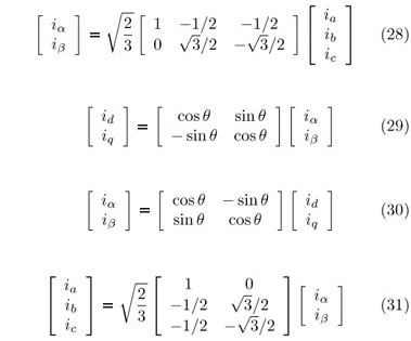
3) Control with PI compensators in the synchronous reference frame - The quality of the three-phase currents synthesis may be significantly improved with the synchronous current controller illustrated in Fig. 12. The transformation of the abc currents to the synchronous dq frame permits to cancel the current steady state error (Buso e Mattavelli, 2006) because the currents in the fundamental frequency become DC quantities. This transformation also gives the controller excellent imunity to integrator saturation caused by offsets in the measured currents. The current controller of Fig. 12 employs two PI compensators for the d and q currents. The dq-abc and abc-dq transformations are presented in the appendix 1 APPENDIX 1 - COORDINATE TRANSFORMATIONS . The transformations employ the angle θ (syncronized with the grid voltages) provided by the phase-locked loop (PLL) of Appendix 2 APPENDIX 2 - DIGITAL THREE-PHASE PLL .
According to the theoretical analysis presented in (Buso e Mattavelli, 2006), the PI compensators of the synchronous frame controller may be designed exactly like the single-phase compensators used in the conventional stationary frame current controller presented in previous section, except that the integral gain of the synchronous frame PI is twice the gain of the conventional single-phase PI. The implementation of the PI compensators used in both stationary and synchronous controllers is explained in Appendix 3 APPENDIX 3 - IMPLEMENTATION OF DIGITAL PI COMPENSATORS .
4.2 Control of the DC link voltage
1) Modeling - The circuit of Fig. 13 shows the DC link capacitor and two equivalent current sources replacing the DC-DC and DC-AC converters. The capacitor receives energy from the DC-DC converter and delivers it to the DC-AC inverter. The difference between the input and output charges increases or decreases the capacitor voltage. The average input and output currents (and consequently the converter input and output powers) must be in equilibrium so that the average capacitor voltage is constant.
The following power balance equations may be written:

where Vac(rms) and Iac(rms) are the per-phase rms grid voltage and current.
Eq. (22) may be simplified considering the average capacitor voltage is approximately constant. Both the capacitor and voltage control time constants are large, so:

From the circuit of Fig. 13 the following average state equation is obtained, considering < iL > = IL:

Because one are interested in finding a small-signal equation of the capacitor voltage and of the converter input current, the assumptions < υlink > = Vlink and < iL > = IL where conveniently used in the average power equation (22) and in the state equation (23), respectively. From (22) and (23):

Replacing < υlink > = Vlink +  link and Iac(pk) =
  ac(pk) +
  ac(pk) in (24) and applying the Laplace transform results the following small-signal s-domain state equation:

From (25) the DC link voltage transfer funcion is obtained:

The transfer function of (26) is consistent with the transfer function developed in (Barbosa et al., 1998), where the authors used a different approach and obtained a similar equation.
2) Control - The controller of Fig. 14 is used to regulate the DC link voltage. The PI compensator with transfer function Cvlk(s) determines the peak of the output sinusoidal currents. Three unit sinusoidal signals synchronized with the grid voltages are multiplied by the PI output Iac(pk). These multiplications generate the current references used by the current controller of section 4.1, Fig. 10. The balance of the input and output powers of the DC link capacitor is achieved by regulating the amplitudes of the sinusoidal currents injected in the grid.
Fig. 15 shows the equivalent control loop of the DC link voltage with the Gvlk(s) transfer function (26) obtained in last section.
With the scheme of Fig. 15 it is possible to design the compensator Cvlk(s) in order to achieve the control of the DC link voltage. With the parameters of Table 4 the following transfer function and compensator (27) are obtained:


The bandwidth of the control loop is made intentionally low so that the DC link voltage control will not cause disturbances in the sinusoidal output currents of the converter. The amplitudes of the currents are regulated so that the average DC link capacitor voltage is constant. The amplitudes of the currents are practically constant when the system is in steady state.
Fig. 16 shows the Bode plots of the equivalent transfer function of the DC link capacitor voltage and of the compensated system. The bandwidth of the control loop is adjusted near 100 Hz with the PI compensator of (27) and the zero located at s = 10 rad/s warranties a low steady state error.
5 SIMULATION RESULTS
This section presents results of simulations of the DC-DC and DC-AC converters. The aim of these simulations is to verify the performance of the controllers and compensators designed in previous sections. The converters where simulated with the parameters of Tables 2-4. The PV array was simulated with the circuit model of Fig. 17 that describes the nonlinear I-V equation (1) presented in section 2. The PV model represents a 6 kW array composed of 2 ×15 KC200GT modules.
5.1 DC-DC converter
The results presented in this section where obtained with the simulation of the FB DC-DC converter fed by the PV array circuit model. The output of the converter is connected to a constant voltage source Vlink = 400 V. The aim of this simulation is to test the behavior of the FB converter with the voltage controller designed in section 3 without the influence of the DC-AC converter and other parts of the system.
Fig. 18 shows the behavior of the PV array voltage Vpv controlled with the voltage compensator designed in section 3. The υpv voltage reaches the reference Vpv,ref = 394.5 V with zero steady state error. Fig. 19 shows the behavior of the PV array current.

5.2 DC-AC inverter
1) Control of the sinusoidal output currents - The simulation result presented in this section was obtained with the DC link capacitor replaced by a constant voltage source Vlink = 400 V. The objective is to analyze the behavior of the current controller of Fig. 10 without the influence of the DC link capacitor and of the rest of the system.
Fig. 20 shows the three-phase currents synthesized by the current controller and injected into the grid through the three coupling inductors connected at the output of the DC-AC inverter (see to Fig. 8).
2) Control of the DC link voltage - The DC-AC converter was simulated separately from the rest of the system. As shown in Fig. (21), in this simulation the DC link capacitor Clink is fed by a current source that is initially zero and steps from 0 to 15 A at t = 0.25 s. This simulation shows that the DC-AC converter and the voltage controller of Fig. 14 keep Clink charged at Vlink,ref. If there is no energy source connected to the capacitor it is charged with energy from the AC grid. When the capacitor is fed by the DC-DC converter (represented by the current source iL in this simulation) the capacitor is charged with part of the input energy. The remainder of energy, that is not stored in the capacitor, is fully delivered as active power to the AC grid.
Figs. 22 and 23 show the DC link voltage and the output currents ia,b,c during this simulation. In Fig. 22 one can see that the DC capacitor charges at the reference voltage of 400 V and after the current step the DC link voltage is reestablished by the voltage controller.
5.3 Complete system with DC-DC and DC-AC converters
In the preceding sections the DC-DC and DC-AC converters where individually simulated and the three control systems (PV array voltage, DC link voltage and sinusoidal output currents) where individually analyzed without the influence of other system parts.
The objective of this section is to present the results of a simulation with all system parts working together: PV array, and DC-DC and DC-AC converters with their respective controllers.
It was shown in section 5.2 that the DC link voltage controller of Fig. 14 is capable to regulate the υlink voltage even in the presence of a large step in the input current. It is now expected that the DC link voltage controller and the DC-AC converter will not significantly suffer influence from the DC-DC converter. Also, from the view point of the DC-DC converter, it is expected that the DC link voltage controller keeps the DC link voltage constant.
Fig. 24 shows the behavior of the DC link voltage υlink and of the υpv during the simulation. The DC link capacitor is initially charged at 300 V. This is necessary because otherwise large transient currents would be drained from the AC grid at the system startup. In a practical system the DC link capacitor is charged either by a rectifier constituted of the DC-AC converter diodes, with a series resistance inserted before the capacitor only during the system startup, or by the DC-DC converter with output voltage control during the startup.
The PV output capacitor Cpv is charged from 0 V to approximately 400 V with energy from the PV array. During the initial charge of the capacitor the PV array supplies its maximum current. Approximately near t = 0.25 s, when the capacitor is charged, the DC-DC converter starts to supply current (iL) to the DC-AC converter, as Fig. 25 shows. The output sinusoidal currents, that where draining power to charge the capacitor Clink, suffer a phase inversion near t = 0.25 s and from this time the DC-AC converter begins to deliver active power to the grid, as Figs. 26 and 27 show.
6 EXPERIMENTAL RESULTS
This section shows some experimental results with the system operating at full load. At the time this paper was written the converter had not been tested with the PV plant and only laboratory experiments were available. The PV array was replaced by a high-power DC source in series with a 6 Ω resistance constituted by a bank of 36 halogen lamps. This experimental DC source permits to make all necessary tests with the converter before it is experimented with the real PV plant.
Fig. 28 shows waveforms of the system operating in steady state with approximately 8 kW of output power. The DC link voltage was set at 500V, the DC input is approximately 280V and the input current is 35A.
Fig. 29 shows the system behavior when submitted to a 6 kW power step. The DC input is suddenly connected and the system reaches steady state in 400ms. The DC input is then removed and the system reaches again steady state (no output power) also in 400ms (observing the DC link voltage perturbation). Fig. 30 shows the three-phase output currents and the DC link voltage in the same situation.
Fig. 31 shows the output current of one phase superimposed with the current reference. Fig. 32 shows the FFT of the output current, where one can see that the 60 Hz component is approximately 30 dB greater than the most significant harmonic component (5 th). No noticeable 3 rd harmonic component is present and the subsequent components above the 5 th are very attenuated.
7 CONCLUSIONS
This paper has presented the modeling and control design of a two-stage PV system based on a DC-DC full-bridge converter and a three-phase grid connected DC-AC inverter. The main objective of the paper was to develop small-signal models and design PI compensators for three purposes: the regulation of the PV voltage, the regulation of the DC link voltage and the injection of purely sinusoidal and synchronized currents into the grid. The simulation results and the experimental results show that the objectives were successfully achieved. Besides presenting the subject of small-signal modeling of the input-regulated DC-DC converter, the paper also serves as a tutorial for the design of the system and several important subjects are carefully analysed: converter modeling, synchronous reference frame current controller, capacitor voltage controller, PV voltage regulation, PLL and implementation of digital anti-windup PI compensators.
ACKNOWLEDGMENTS
This work was sponsored by FAPESP, CNPq, and CAPES.
Artigo submetido em 04/12/2009 (Id.: 01090)
Revisado em 13/04/2010, 31/08/2010
Aceito sob recomendação do Editor Associado Prof. Darizon Alves de Andrade
The digital PLL of Fig. 33 is a simplified version of the PLL presented in (Marafão et al., 2005) (Kubo et al., 2006) (Marafão et al., 2004). The principle of operation is the dot product between the voltage vector v and the orthogonal vector u⊥. When the PLL is synchronized with the grid voltages the two vectors are orthogonal and the product is zero. The PI compensator works to minimize the error ε = 0 v · u⊥, i.e. to cancel the dot product, and generates the correction component Δω. The integration of the angular frequency ω = Δω + ω0 gives the angle θ⊥. The vector u1 corresponds to the unitary sinusoids synchronized with the positive sequence of the grid voltages. A sequence detection algorithm (not shown here) is used to generate the output signals in the correct phase sequence. This algorithm is based on the abc-αβ transformation and detects the sequence (positive or negative) by observing the direction (clockwise or counterclockwise) of the rotating voltage vector.
The continuous-time compensators designed in previous sections can be realized as discrete-time digital compensators. There are several ways of discretizing analog compensators. All of them present similar results when the compensator bandwidth is not greater than 10% of the sampling frequency (Franklin et al., 1995). The Tustin or bilinear transform is used in this work. The compensators and controllers were implemented with the Texas floating point digital signal controller TMS320F28335 with sampling frequency s = 1/Ts = 10 kHz.
A discrete-time compensator is a digital filter. The filter coefficients may be obtained from the s-domain transfer function with the desired transformation method. In MATLAB the following command may be used to find the filter coefficients: [numz, denz] = bilinear(nums, dens, fs), where numz = [b0b1] and denz = [a0a1] are the numerator and denominator vectors with the coefficients of the Tustin (or bilinear) approximation.
In the IIR direct transposed form the filter difference equation is (Oppenheim e Schafer, 1989):

The difference equation (32) is the simplest way to implement the PI compensator. The proportional and integral components are embedded in the equation. In order to implement the simple anti-windup strategy proposed in this paper, one wish to develop another equation.
The following equation describes a PI compensator:

with the trapezoidal integrator ik:

The compensator of (33) and (34) is equivalent to the compensator described by (32), with the difference that in (33) the proportional and integral parts are separated.
One can write the past integrator value ik-1 as:

so ik can be rewritten as:

Replacing (36) in (33), the difference equation (32) becomes:

The above equation (37) shows the correspondence between the coefficients of (33) and (32), with a1 = 1. The difference equations (33) and (32) may be used indistinctly to implement the first order PI compensator. However, in the form of (33) the simple anti-windup algorithm of Fig. 34 is possible. This algorithm simply stops the integrator when the control output exceeds the limits. In practical systems the compensator output may sometimes exceed the maximum effective control effort. This causes integrator saturation and deteriorates the control performance.
- Barbosa, P. G., Rolim, L. G. B., Watanabe, E. H. e Hanitsch, R. (1998). Control strategy for grid-connected DC-AC converters with load power factor correction, Generation, Transmission and Distribution, IEE Proceedings-, Vol. 145, pp. 487-491.
- Buso, S. e Mattavelli, P. (2006). Digital control in power electronics, Morgan & Claypool Publishers.
- de Souza, K. C. A., Coelho, R. F. e Martins, D. C. (2007). Proposta de um sistema fotovoltaico de dois estágios conectado à rede elétrica comercial, Revista Eletrônica de Potência (SOBRAEP), Brazilian Journal of Power Electronics 12(2): 129-136.
- Erickson, R. W. e Maksimovic, D. (2001) . Fundamentals of Power Electronics, Kluwer Academic Publishers.
- Franklin, G. F., Powell, J. D. e Emami-Naeini, A. (1995). Feedback control of dynamic systems
- Kubo, M. M., Villalva, M. G., Marafăo, F. P. e Ruppert F., E. (2006). Análise e projeto de PLL de desempenho melhorado baseado em filtro passa-baixas chebyshev inverso, 16th Brazilian Conference on Automatic Control, CBA
- Kyocera (n.d). KC200GT high efficiency multicrystal photovoltaic module (datasheet).
- Marafăo, F. P., Deckmann, S. M., Pomilio, J. A. e Machado, R. Q. (2004). A software-based PLL model: Analysis and applications., Congresso Brasileiro de Automática, CBA, Brazilian Conference of Control and Automation
- Marafăo, F. P., Deckmann, S. M., Pomilio, J. A. e Machado, R. Q. (2005). Metodologia de projeto e análise de algoritmos de sincronismo PLL, Revista da Sociedade Brasileira de Eletrônica de Potęncia (SOBRAEP), Brazilian Journal of Power Electronics 10(1).
- Middlebrook, R. (1988). Small-signal modeling of pulse-width modulated switched-mode power converters, Proceedings of the IEEE 76(4): 343-354.
- Middlebrook, R. D. e Cuk, S. (1976). A general unified approach to modelling switching converter power stage, IEEE Power Electronics Specialists Conference, pp. 18-34.
- Oppenheim, A. V. e Schafer, R. (1989). Discrete-Time Signal Processing
- Villalva, M. G., Gazoli, J. R. e Ruppert F., E. (2009a). Comprehensive approach to modeling and simulation of photovoltaic arrays, IEEE Transactions on Power Electronics 25(5): 1198-1208.
- Villalva, M. G., Gazoli, J. R. e Ruppert F., E. (2009b). Modeling and circuit-based simulation of photovoltaic arrays, Revista Eletrônica de Potência (SOBRAEP), Brazilian Journal of Power Electronics
- Villalva, M. G. e Ruppert F., E. (2007). Buck converter with variable input voltage for photovoltaic applications, Congresso Brasileiro de Eletrônica de Potência (COBEP)
- Villalva, M. G. e Ruppert F., E. (2008a). Dynamic analysis of the input-controlled buck converter fed by a photovoltaic array, Revista Controle & Automação - Sociedade Brasileira de Automática, Brazilian Journal of Control and Automation 19(4): 463-474.
- Villalva, M. G. e Ruppert F., E. (2008b). Input-controlled buck converter for photovoltaic applications: modeling and design, 4th IET Conference on Power Electronics, Machines and Drives. PEMD, pp. 505-509.
APPENDIX 1 - COORDINATE TRANSFORMATIONS
APPENDIX 2 - DIGITAL THREE-PHASE PLL
APPENDIX 3 - IMPLEMENTATION OF DIGITAL PI COMPENSATORS
Publication Dates
-
Publication in this collection
19 July 2011 -
Date of issue
June 2011
History
-
Received
04 Dec 2009 -
Reviewed
13 Apr 2010 -
Accepted
31 Aug 2010


