Abstract
Hexametildisilazane (HMDS) plasma polymerized thin films obtained using low frequency power supplies can be used to make adsorbent films and turn surfaces hydrophobic. The aim of this work was to verify the hydrophobicity and adsorption properties of HMDS thin films (with and without the addition of oxygen, resulting in double or single layer films) obtained using an inductive reactor powered with a 13.56 MHz power supply. Single and double layer thin films were deposited on silicon for film characterization, polypropylene (PP) for ultraviolet (UVA/UVC) resistance tests, piezoelectric quartz crystal for adsorption tests. The double layer (intermixing) of HMDS plasma polymerized films and HMDS plasma oxidized surfaces showed a non-continuous layer. The films showed good adhesion to all substrates. Infrared analysis showed the presence of CHn, SiCH3, SiNSi and SiCH2Si within the films. Contact angle measurements with water showed hydrophobic surfaces. UVA/UVC exposure of the films resulted in the presence of cross-linking on carbonic radicals and SiCH2Si formation, which resulted in a possible protection of PP against UVA/UVC for a duration of up to two weeks. Adsorption tests showed that all organic reactants were adsorbed but not water. Plasma etching (PE) using O2 showed that even after 15 minutes of exposure the films do not change their hydrophobic characteristic but were oxidized. The results point out that HMDS films can be used: for ultraviolet protection of flexible organic substrates, such as PP, for sensor and/or preconcentrator development, due to their adsorption properties, and in spatial applications due to resistance for O2 attack in hostile conditions, such as plasma etching.
plasma polymerization; sensor membrane; surface protection
Hydrophobic plasma polymerized hexamethyldisilazane thin films: characterization and uses
Alexsander Tressino de CarvalhoI; Rodrigo Amorim Motta CarvalhoI; Maria Lúcia Pereira da SilvaI, * * e-mail: malu@usp.br ; Nicole Raymond DemarquetteII
IDepartamento de Sistemas Eletrônicos, Escola Politécnica,Universidade de São Paulo, Av. Prof. Luciano Gualberto, travessa 03, 158, Sala A1 46, 05508-900 São Paulo - SP, Brazil
IIDepartamento de Engenharia de Materiais (PMT), Escola Politécnica, Universidade de São Paulo, 05508-900 São Paulo - SP, Brazil
ABSTRACT
Hexametildisilazane (HMDS) plasma polymerized thin films obtained using low frequency power supplies can be used to make adsorbent films and turn surfaces hydrophobic. The aim of this work was to verify the hydrophobicity and adsorption properties of HMDS thin films (with and without the addition of oxygen, resulting in double or single layer films) obtained using an inductive reactor powered with a 13.56 MHz power supply. Single and double layer thin films were deposited on silicon for film characterization, polypropylene (PP) for ultraviolet (UVA/UVC) resistance tests, piezoelectric quartz crystal for adsorption tests. The double layer (intermixing) of HMDS plasma polymerized films and HMDS plasma oxidized surfaces showed a non-continuous layer. The films showed good adhesion to all substrates. Infrared analysis showed the presence of CHn, SiCH3, SiNSi and SiCH2Si within the films. Contact angle measurements with water showed hydrophobic surfaces. UVA/UVC exposure of the films resulted in the presence of cross-linking on carbonic radicals and SiCH2Si formation, which resulted in a possible protection of PP against UVA/UVC for a duration of up to two weeks. Adsorption tests showed that all organic reactants were adsorbed but not water. Plasma etching (PE) using O2 showed that even after 15 minutes of exposure the films do not change their hydrophobic characteristic but were oxidized. The results point out that HMDS films can be used: for ultraviolet protection of flexible organic substrates, such as PP, for sensor and/or preconcentrator development, due to their adsorption properties, and in spatial applications due to resistance for O2 attack in hostile conditions, such as plasma etching.
Keywords: plasma polymerization, sensor membrane, surface protection
1. Introduction
HMDS is a reactant commonly used for different applications. In wet processes is used for volatile derivativation of a large variety of biological compounds1-4 or surface silylation5-8 in microelectronic applications, and for surface preparation of the chromatographic capillary columns9. In dry processes is normally used for plasma processing in microelectronic, for several applications, such as surface protection10,11 and optics12-14.
HMDS plasma polymerization was extensively studied using different frequencies power supplies, but only films with low amount of carbon radicals are normally used, such as for surface protection15-17. Recently, other applications for plasma HMDS thin films have arisen due to the interesting properties that films with high amount of carbon demonstrate such as high hydrophobicity, resistance to UV radiation, acid and bases etching and adhesion to several substrates18-20. This high hydrophobicity originates from the high amount of CH3 species within the film, which also induces an easy adsorption of organic compounds21,22 and ultraviolet protection20. However these films were obtained using capacitive reactors powered using a 40 kHz power supply.
The aim of this work is to verify if HMDS plasma polymerized thin films produced in an inductive tubular plasma reactor coupled with 13.56 MHz power supply presented the same adsorption and protection characteristics found with 40 KHz power supply. For comparison, wet depositions on ligno cellulose surfaces were also carried out.
2. Experimental
All reactants used were P.A., with the exception of HMDS reactant that was industrial grade. The substrates used were: silicon wafers (3", <100> 10-20 Wcm), piezoelectric quartz crystals (PQC) with frequency of 4.096 MHz, polypropylene and Lignocellulosic samples, in particular beans from Cerealista Cristo Rei Ltda. Beans were used due to theirs high degasification rate that favor changes on HMDS film characteristics.
HMDS wet process used two different procedures: exposure to saturated HMDS vapor atmosphere or HMDS dip23. HMDS plasma deposition used a tubular reactor described elsewhere24. Figure 1 shows the reactor used in this work.
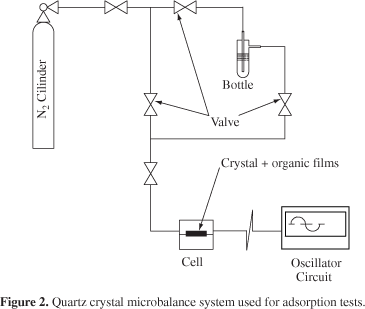
Silicon wafer was used for HMDS plasma polymerized film characterization. Therefore during plasma deposition on all substrates, silicon wafer was used as reference. The films deposited on silicon were characterized by perfilometry, to determine deposition rate, infrared spectroscopy, to analyze the main chemical species within the films, and measuring the contact angles formed by drops of distillate water. The films deposited on PQC were tested for adsorption using a quartz crystal microbalance (QCM). The adsorption tests used organic compounds in large range polarity. Figure 2 shows the QCM system used for adsorption test. The films deposited on polypropylene were tested for their ability to protect this polymer from UV radiation: 8 W, UVA and UVC Lights were maintained about 10 cm apart from the polypropylene during several weeks. The chemical modification of the samples was evaluated visually, by immersion in water, contact angle measurement, FTIR and Vickers tests were also carried out.
The films deposited on beans were tested for their resistance to acid and basic solutions and also for other characteristics as follows:
-
Etch resistance and aging: For etching tests grains were immersed in aqueous solutions in a large range of pH [HCl (pH ~ 0); H
2SO
4 (pH ~ 3); H
2O (pH ~ 6); NH
4OH (pH ~ 9); NaOH (pH ~ 14)]. After five minutes, the surface was evaluated by optical microscopy. The procedure was repeated until the surface showed any change. For aging tests, the grain was immersed in water for 30 minutes and its surface evaluated by optical microscopy. After four months the procedure was repeated. Theses tests were carried out only for plasma polymerized films;
-
Reaction with water at room temperature and at boiling point: The grains were immersed approximately for 40 minutes then their surface was evaluated by optical microscopy;
-
Humidity resistance: Treated and untreated grains were kept in a dissecator with water for 10 days at 10 mTorr imitating very humid weathering condition during storing. Optical microscopy was used to evaluate the surface of the beans, as described for etching resistance tests; and
-
Resistance to UV: The grains were monitored continuously, visually, by immersion in water and using contact angle measurement.
3. Results and Discussion
The results are showed in two sections: 1) production and characterization of HMDS plasma polymerized films and 2) Tests of adsorption and surface protection.
3.1. Production and characterization of HMDS plasma polymerized films
HMDS plasma polymerized films obtained on silicon wafers showed the following characteristics25:
-
Non rigid (verified by scratching test);
-
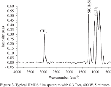
Deposition rates ranging from 200 to 700 Å/min when power and pressure varied from 200 to 600 W and 0.2 to 1.5 Torr, respectively with a maximum deposition rate for 0.3 Torr and 400 W. Depositions rates were higher at the center of the electrode (position B);
-
Mostly formed by of SiCH
3; SiCH
2Si and SiNSi bonds. A typical FTIR spectrum of the film is shown in
-
Water contact angles of roughly 90°; and
-
Resistance to acid and basic solutions. However, at pH 14 optical microscopy analysis showed surface modification in small spots, probably due to partial etching.
The most hydrophobic films obtained with high SiCH3 relative intensity and good etching resistance for acid and basic solutions were chosen for adsorption and surface protection tests. These films were produced at 0.3 Torr, 400 W, 5 minutes and thickness was approximately 3000 Å.
In order to improve the HMDS plasma polymerized films mechanical resistance, intermixing depositions were carried out using oxygen to form a second layer on the film. This second layer might be rigid because HMDS + O2 plasmas easily form silicon oxide thin films13. Four different procedures as described in Table 1 were tested. When following procedures 1, 2 and 4 oxygen was added to the plasma to form the second layer (silicon oxide). When following procedure 4 the second layer was formed only by oxidation. Procedure 3 was adopted to evaluate the interface between the layers. Infrared spectra showed silicon oxide formation when following procedure 3 but the low deposition rate obtained in that case indicates that the intermixing most likely lead to a thin film formed at the interface between the layers. Likewise, when following procedure 4 a very thin silicon oxide film was formed at the surface of the HMDS plasma polymerized film. Whereas infrared spectra for samples obtained following procedures 1 and 2 show low amount of SiOSi species, the films obtained following procedure 4 contained a high amount of SiOSi. Therefore, the bombardment of oxygen that occured when following procedure 4 probably allowed oxide formation in an easier fashion than when using plasma HMDS+O2 reactions. These results are in good agreement with deposition rates results commented above.
Figure 4 shows a typical aspect of a film obtained when following procedure 4, as described on Table 1. Small structures with a needle shape (see arrow on the photograph) can be observed. These irregularities indicate that the intermixing procedures probably did not favor, in this case, a silicon oxide continuous layer formation. Therefore, the mechanical resistance will be improved, but only in a small range, as verified using Vickers tests.
Thus, although HMDS plasma polymerized films show good properties when exposed to severe chemical conditions (acid and basic solutions), the film is not rigid and has low mechanical resistance, as verified by scratching test.
3.2. Tests of adsorption and surface protection
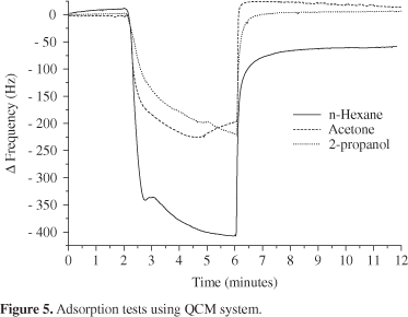
HMDS plasma polymerized films were deposited on PQC and adsorption tests were carried out. Figure 5 shows a typical result for film obtained with high amount of SiCH3 (0.3 Torr, 400 W, 3000 A) species. As can be seen in Figure 5, films are adsorbent for organic compounds, polar and non-polar. These results are similar to the ones obtained when using a planar reactor powered by a low frequency power supply12.
Resistance and reproducibility tests were also carried out using QCM and with the same organic compounds used for adsorption tests. In this test the compound is admitted and removed periodically (1 minute for admission or removal) and possible variations of frequency are recorded. Only nitrogen flows in the cell during the removal of the compound. The HMDS plasma polymerized film showed good resistance to the organic compounds tested. However, for acetone and after several cycles (more than 10 times) changes could be noticed of the film behavior. This behavior is most likely due to non-gravimetric interactions, such as swelling of the film. Figure 6 shows typical results for 2-propanol and acetone.
Figure 7 shows infrared spectra of HMDS films before and after eight days exposure to UVC. It can be seen that after ultraviolet exposure (UVA or UVC) SiCH3 species cross-link and/or oxidize, leading to SiCH2Si or SiOSi formation. These results are similar to the ones found using planar reactor at 40 KHz power supply20.
Polypropylene samples were also treated with HMDS plasma films and exposed to ultraviolet radiation (UVA and UVC) and the infrared spectra were evaluated during 30 days. It was noticed that treated samples resist to ultraviolet for a longer time than the untreated ones. After 15 days of UVC radiation, the relative intensity of the main species did not change for the treated ones but for the untreated (approximately 16% variation relative intensity). Moreover, Vickers measurements showed lower values for untreated samples (approximately 10% lower).
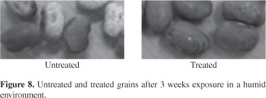
HMDS plasma films were also deposited on grains for tests of surface protection. The deposition occurred without any difficulty, but the high degasification rate of the grains demanded approximately thirty minutes to reach the ultimate pressure (10 mTorr). However no difference between the films obtained when depositing on grains and films deposited on other substrates were observed as can be proven by the analysis of the silicon wafer that were inserted in the reactor together with the grains and used as reference. The treated grains were hydrophobic, as verified by water contact angle measurements, and resistant to water immersion, at room temperature or boiling point, up to 20 minutes. After four months, the same behavior was found. For humidity test, after 10 days the treated grains showed no alteration but the untreated presented microorganisms on the surface, as can be see in Figure 8. Whereas microorganisms were found at the surface of untreated grains approximately after a week of water vapor exposure in the case of treated grains those microorganisms occurred after only three weeks. The grains were also exposed to ultraviolet radiation during 21 days. After the exposure the grains were tested for immersion in water and humid environment. It was verified the same behavior found for the treated grains without exposure. Therefore, the film does not change its characteristics significantly but some color variation may occur after the exposure, probably due to partial interaction with ultraviolet radiation.
For comparison, grains were treated with HMDS using wet process. The two procedures exposure to HMDS vapor or dip in HMDS showed the same behavior. The main difference observed was on the grain color most likely due to sililation. Immersion in water at room temperature requires only five minutes for adsorption occurs. Humid environments also favor microorganism attack after one week, similar to the results obtained with untreated grains. Therefore, the monolayer formed for HMDS wet reaction is not suitable for surface protection, such as during storage.
4. Conclusions
Plasma polymerized HMDS films with high amount of SiCH3 species show hydrophobic character and adsorption properties that indicate them for polymeric surface protection, especially against water. Therefore, these films can be useful for grain protection during storage.
The cross-link reaction during ultraviolet exposure also indicates these films for surface protection in severe conditions, such as outer space uses where the amount of UV light is especially high. The adsorption characteristics could be useful for sensor development; however, the low mechanical resistance of these films can be a drawback and must be addressed. Moreover, these films were obtained using clean technologies and environmentally friendly reactants.
Acknowledgments
The authors would like to thank Pedro Ortiz for Vickers tests, Instituto de Química da Universidade de São Paulo for QCM measurements CNPq and FAPESP for financial support.
Received: December 2, 2004; Revised: July 13, 2005
- 1. Merck Catalog 1990; 13: p. 4708.
- 2. Beil. Encyclopedia 1948; 4(IV): p. 4014.
- 3. Nouvel C, Ydens I, Degee P, Dubois P, Dellacherie E, Six JL. Partial or total silylation of dextran with hexamethyldisilazane. Source: Polymer 2002; 43(6):1735-1743.
- 4. Firouzabadi H, Sardarian AR, Khayat Z, Karimi B, Tangestaninejad S. Nitrogen ligand complexes of metal chlorides as effective catalysts for the highly regio- and chemoselective silylation of hydroxyl groups with hexamethyldisilazane (HMDS) at room temperature. Synthetic Communications 1997; 27(15):2709-2719.
- 5. Catalog Handbook of Fine Chemicals, Aldrich, nş H1,000-2.
- 6. Tillu VH, Jadhav VH, Borate HB, Wakharkar RD. Solvent free selective silylation of alcohols, phenols and naphthols with HMDS catalyzed by H-beta zeolite. Arkivoc 2004; 14:83-88.
- 7. Schneider H, Puchta GT, Kaul FAR, Raudaschl-Sieber G, Lefebvre F, Saggio G, et al. Immobilization of eta(5)-cyclopentadienyltris(dimethylamido) zirconium polymerization catalysts on a chlorosilane- and HMDS-modified mesoporous silica surface: a new concept for supporting metallocene amides towards heterogeneous single-site-catalyst. Journal Of Molecular Catalysis A-Chemical 2001 May; 70(1-2):127-141.
- 8. Xie B, Muscat AJ. Silylation of porous methylsilsesquioxane films in supercritical carbon dioxide. Microelectronic Engineering 2004 Oct; 76(1-4):52-59.
- 9. Chromatography Products for analysis and purification, Supelco Chromatography 2001; 10.
- 10. Mex L, Kramer A, Francke C, Muller J Source; Plasma polymerized hexamethyldisilasane for the passivation of YBa2Cu3O7-x devices; Superconductor Science & Technology 1998 Apr; 11(4): 426-432.
- 11. Francke C, Mex L, Kramer A, Meyer B, Muller J. Source Large area flux transformers and passivation for flip-chip magnetometers. IEEE Transactions On Applied Superconductivity 1997 Jun; 7(2):2768-2771.
- 12. da Silva MLP, Tan IH, Nascimento AP. Use of plasma polymerized highly hydrophobic hexamethyldissilazane (HMDS) films for sensor development. Sensors Actuat Chemical 2003 Jun; 91(1-3): 362-369.
- 13. Lee HR, Kim DJ, Lee KH. Anti-reflective coating for the deep coloring of PET fabrics using an atmospheric pressure plasma technique. Surf Coat Tech 2001 Jun; 142:468-473.
- 14. Johnson EM, Clarson SJ, Jiang H, et al. Plasma polymerized hexamethyldisiloxane (HMDS) barrier layers. Polymer 2001 Jul; 42(16):7215-7219.
- 15. D'agostino R. Plasma Deposition The Treatment And Etching Of Polymers. Centro Di Studio Per La Chimica Dei Plasmi, Cnr, University Of Bari. Academic Press Published 1990 Nov; p. 44.
- 16. Lim SC, Kim SH, Lee JH, Kim MK, Kim DJ, Zyung T. Surface-treatment effects on organic thin-film transistors. Synthetic Metals 2005 Jan; 148(1):75-79.
- 17. Ohgishi A, Motoyama S, Sawai M, Tatsuta T, Tsuji. Deposition of cathode coupled plasma enhanced chemical vapor deposition SiN films using liquid source material. Japanese Journal Of Applied Physics Part 2-Letters 2003 Sep; 42(9AB):L1090-L1092.
- 18. Silva MLP, Demarquette NR, Tan IH. Use of HMDS/Hexane double layers for obtaining low cost selective membrane. Cellulose. 2003; 10:171-178.
- 19. Tan IH, Silva MLP, Demarquette NR. Paper surface modification by plasma deposition of double layers of organic silicon compounds. J. Mater. Chem. 2001; 11:1019-1025.
- 20. Pereira GJ, Silva MLP, Tan IH, Gouvea D. Modification of surface properties of alumina by plasma treatment. J. Mat. Chem. 2000; 20:1-3.
- 21. Nogueira S. Caracterização de filmes obtidos a partir da deposição por plasma de hexametildissilazana [Dissertação de Mestrado]. EPUSP; 2000.
- 22. Nascimento Filho AP. Produção de novos filmes para detecção de poluentes [Dissertação de Mestrado]. EPUSP; 2002.
- 23. Carvalho AT, Carvalho RAM, Silva MLP, Demarquette, NR. HMDS plasma polymerized films: production and use for surface protection. 6ş Congresso Brasileiro De Polímeros/ IX International Macromolecular Colloquium, Gramado. 2001.
- 24. Tan IH, Demarquette N, Silva MLP, Degasperi FT, Dallacqua R. Adhesion improvement of cellulose to polypropylene: a comparison of plasma treatment o PP and plasma deposition on cellulose. ISPC-14 Symposium proceedings, 1999; pp. 1907.
- 25. Carvalho AT. Produção de filme hidrofóbico para proteção de superfície: utilização na estocagem de grãos [Monografia]. FATEC; 2002.
Publication Dates
-
Publication in this collection
10 Apr 2006 -
Date of issue
Mar 2006
History
-
Accepted
13 July 2005 -
Received
02 Dec 2004